|
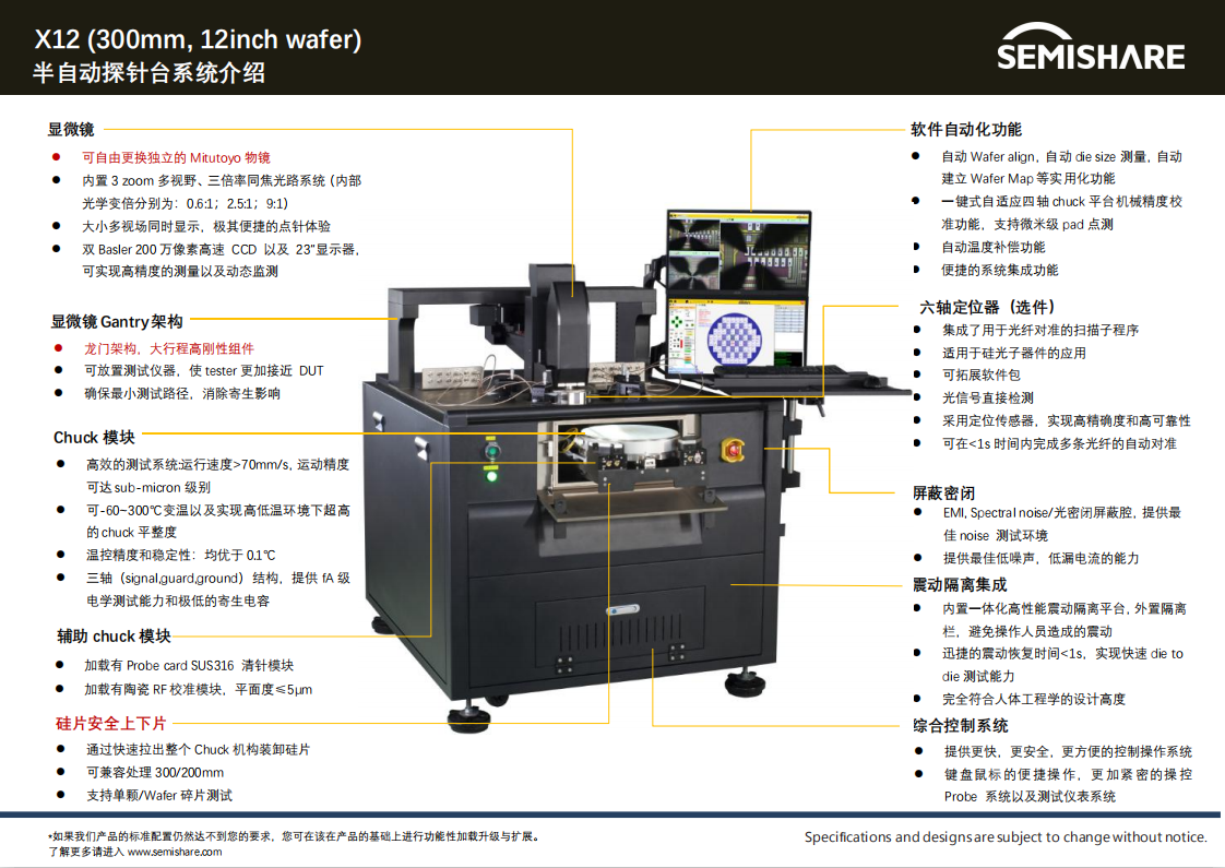
SX Series Semi-automatic Wafer Probe Station
|
|
Specification
|
|
Model
|
SX-6
|
SX-8
|
SX-12
|
|
Dimension(W*L*H)
|
1000mm * 1400mm * 1400mm
|
1100mm * 1500mm * 1400mm
|
1200mm * 1600mm * 1400mm
|
|
Weight(about)
|
1000KG
|
1150KG
|
1350KG
|
|
Electricity Demand
|
AC220V,50~60Hz
|
|
CDA demand
|
0.4~0.8Mpa
|
|
Chuck
|
Size
|
6″
|
8″
|
12″
|
|
X-Y Travel range
|
200mm * 300mm
|
250mm * 400mm
|
350mm * 500mm
|
|
X-Y Resolution
|
0.1μm
|
|
X-Y Repeatability
|
≤±1μm
|
|
X-Y Move speed
|
≥70mm/sec
|
|
Z Travel range
|
20mm
|
|
Z Resolution
|
0.1μm
|
|
Z Repeatability
|
≤±1μm
|
|
Z Move speed
|
≥20mm/sec
|
|
Theta Travel range
|
±10°
|
Theta resolution
|
0.0001°
|
|
Sample Fixed mode
|
Vacuum adsorption , Independent control
|
|
Sample Exchange
|
Chuck quickly roll out for wafer fast exchange.
|
|
Structure
|
Triaxial ultra-low noise design,Gold plating, Chuck surface is electrical floating
|
|
Platen
|
Specifications
|
O shape platen, 12 micropositioners available(When the octagon box is not installed)
|
|
Microscope
X-Y-Z
|
X-Y Travel range
|
2″* 2″
|
|
X-Y Resolution
|
0.1μm
|
|
X-Y Repeatability
|
±2μm
|
|
X-Y Move speed
|
≥10mm/sec
|
|
Z Travel range
|
5″
|
|
Z Resolution
|
0.1μm
|
|
Z Repeatability
|
≤ ±1μm
|
|
Z Move speed
|
≥10mm/sec
|
|
Microscope
|
Variable magnification microscope
|
Zoom:15:1,Three gears and could display low(0.6X) and high(2.5X or 9X)
|
|
magnification in the same time
|
|
Camera
|
Double cameras(200W or 500W Industrial digital camera)
|
|
Micropositioner Specification
|
Mechanical resolution
|
10μm / 2μm / 0.7μm
|
|
X-Y-Z Move range
|
13mm-13mm-13mm
|
|
Current leakage
|
10pA / 100fA / 10fA
|
|
Connector type
|
Banana plug adapter/Coaxial /Three-axis/ SMA /SHV etc.
|
|
Base
|
Magnetic/vacuum adsorption base
|
|
Temperature
specification
|
Temperature range
|
﹣60℃-200℃ (Standard), other Temperature range upon request
|
|
Temperature stability
|
±0.1℃
|
|
Tmeperature resolution
|
0.01℃
|
|
Heating time(12″chuck)
|
﹣60℃ to +25℃ ≤ 10min
|
|
+25℃ to +200℃ ≤10 min
|
|
Cooling time(12″chuck)
|
﹢200℃ to +25℃ ≤ 12min
|
|
﹢25℃ to -60℃ ≤ 25min
|
|
Noise
|
<60dB
|
|
Heating method
|
Low Voltage DC(LVDC)/PID control
|
|
Refrigeration method
|
Refrigeration compressor
|
|
Anti-Vibration
|
Anti-Vibration method
|
Air film anti-vibration system,Ensure nonvisible vibration in the screen
|
|
when the microscope zooming in at 2000X
|
|
Vibration suppression
|
In the process of chuck movement, it can be extremely fast to ensure the
|
|
stability of the chuck ≤1S, Improve the test efficiency.
|
|
system mask
|
EMI shielding
|
> 30 dB (typical) @ 1 kHz to 20GHz
|
|
Light attenuation
|
≥ 130 dB
|
|
Spectral noise floor
|
≤ -180 dBVrms/rtHz
|
|
System AC noise
|
≤5 mVp-p (≤ 1 GHz)
|
|
Software function
|
|
Automatic wafer alignment
|
Automatic wafer height measurement and compensation
|
|
Automatic Die size measurement and auto mapping
|
Wafer map edit arbitrary
|
|
Demarcate difference data with Ink mark
|
Real-time test results display
|
|
Easy data management of the instrument input/output
|
The test results can be divided into different bin values
|
|
Multi tester fast integration , support both single Die testing and continuous testing
|
Support Z, N shape test
|
|
One touch automatic RF calibrate and probe tips cleaning
|
Separation of OS and application software, can be upgraded independently.
|
|
Robust data storage and processing capabilities
|
Automatic data and curves storage and remote access
|
|
Communication interface:R232/485/TCP/IP/GPIB
|
|
|
Characteristic
|
|
Ultrahigh test accuracy, efficiency and stability
|
Convenient tester integration
|
|
Mult magnification simultaneous display optical system
|
High power wafer test Upgradable
|
|
-60~200℃ super low noise chuck
|
RF test Upgradable
|
|
Feature-rich test software.
|
Fully automatic wafer test Upgradable
|


